On-chip Optical Phase Monitoring in Multi-Transverse-Mode Optical Processors (MTMOP)
Programmable optical processors are promising structures for ultrafast and energy efficient optical computation.
These processors can replace conventional electronic processors to efficiently perform the vector-matrix multiplication portion of neural networks,
integrated microwave photonics (IMWP), and other applications such as multiply-accumulate (MAC) operation in computing.
This is due to the inherent parallelism presents in optics in contrast with sequential operations in electronics.
Energy efficient computational accelerators in silicon photonic technology allow better scalability meeting the computational demands of future machine learning applications.
Calibrating and programming the optical processors remain challenging due to challenges related to phase error caused by fabrication variations and complexities in the measurement of optical phase.
Phase setting incertitude translates into computation error and accuracy. Developing an accurate and practical calibration/programming scheme is a key step towards achieving scalable programmable optical processors.
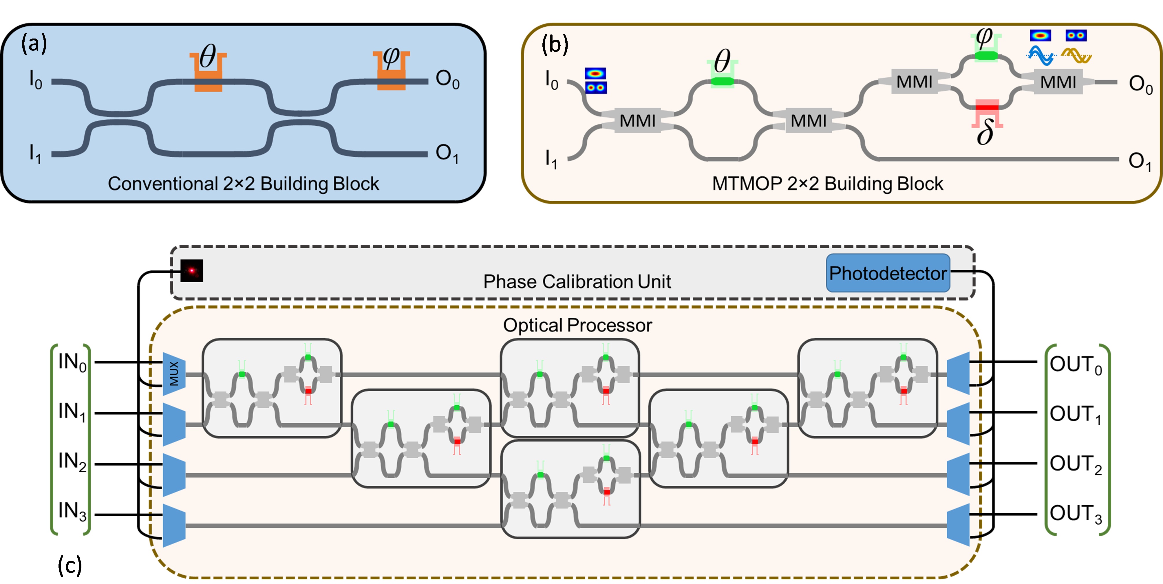
For the first time, we propose the Multi-Transverse-Mode Optical Processors (MTMOP) for optical computing applications. This is a novel architecture exploiting multiple transverse modes in an optical computation platform.
The advantage of the MTMOP is its accurate, low-cost, and fast programming/calibration procedure.
In a conventional programmable optical processor, one needs a coherent detector to measure the optical phase of phase shifters to calibrate/program the processor and train the neural network.
Using coherent detectors drastically increases the cost and complexity of the optical processor programmability.
Using MTMOP, we overcome this challenge by introducing a new but simple building block enabling optical phase measurement without the need for coherent detection.
Using orthogonal optical modes, the MTMOP includes a design that converts the optical phase into optical intensity that can then be easily measured using optical photodetectors.
Please see more details here.
Fabrication of AlGaN/GaN and AlInGaN/GaN Hetero-structure field effect transistors (HFETs) at McGill Nanotools-Microfab lab (mnm), using optical lithography and electron-beam lithography
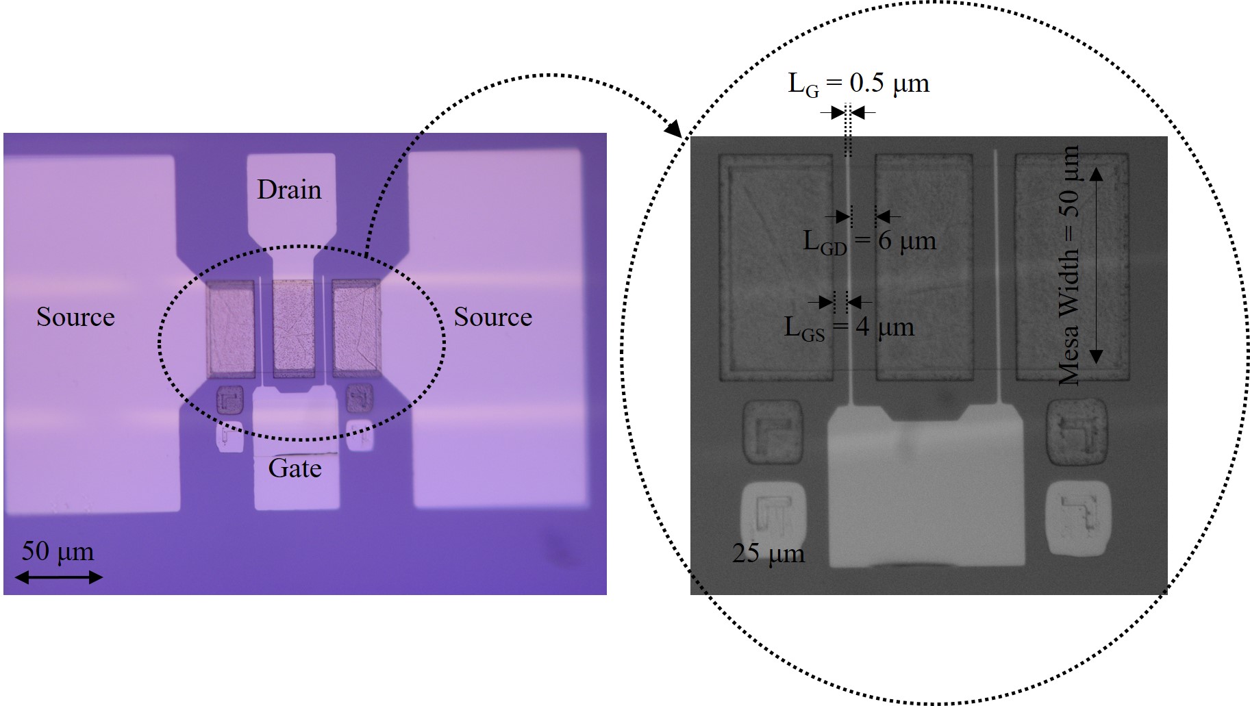
A process recipe has been developed for the microfabrication of submicron gate AlGaN/GaN heterojunction field effect transistors (HFETs) using electron beam lithography at McGill’s nanotools micro-fabrication (MNM) lab. This is the first transistor with submicron feature size fabricated using electron beam lithography at MNM. This project provides MNM with the ability of fabricating electronic semiconductor devices with submicron feature size using electron beam lithography. The fabricated transistors were characterized at Concordia Reliable Electron Devices research lab, and superb characteristics were observed: maximum drain current density of 557 mA/mm, extrinsic gate transconductance of 140 mS/mm, subthreshold swing as low as 107 mV/dec and Ion/Ioff ratio as high as 3.7×10⁷.
Study of Gate-Leakage in III-nitride HFETs
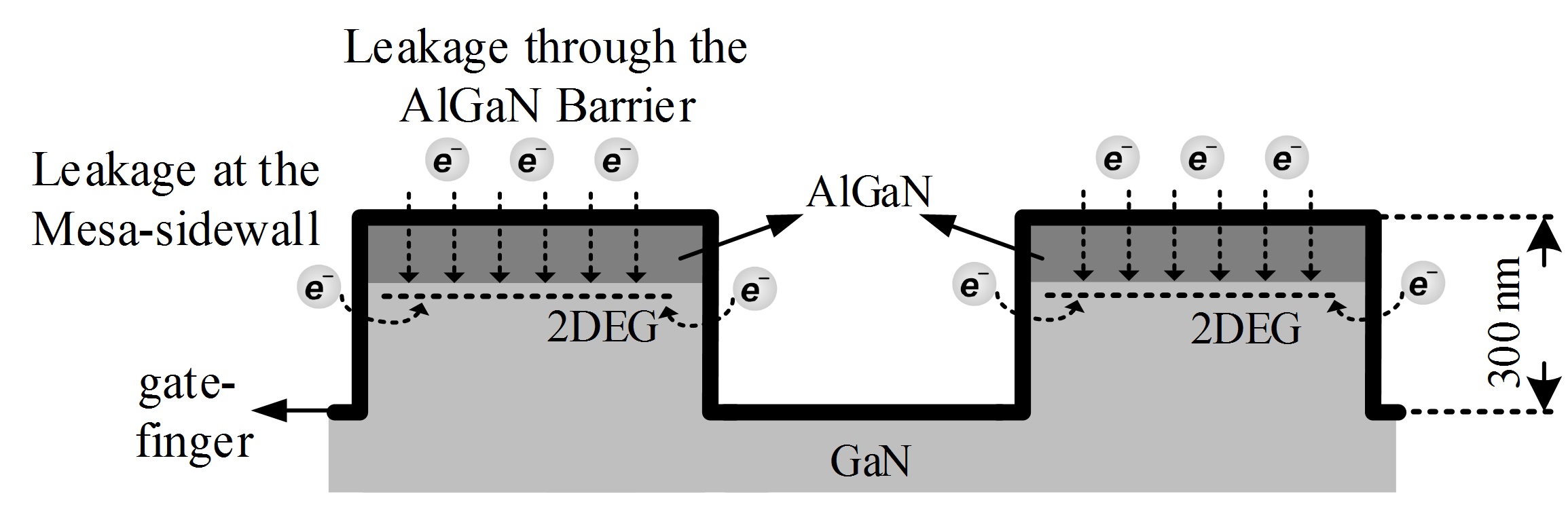
A comprehensive model considering different leakage paths for describing the reverse gate leakage in GaN HFETs has been presented. The first novel contribution of this model is providing evidences into the existing a leakage path between the gate and the channel at the sidewall of mesa (the feature where the transistor is built on to be isolated from the adjacent transistors). This leakage path which is identified for the first time has been widely neglected in previous studies. The second novel contribution of this model is that, it demonstrates that the electron tunneling takes place through only a small portion of the gate, which boasts the highest electric field or the smallest Schottky barrier height. By applying the presented theory, the origin of the inconsistencies inherent to the previously similar presented models in selecting the unrealistic values of model parameters could be explained for the first time. The outcomes of this research project have been published in t wo papers in IEEE Transactions on Electron Devices on Apr. 2016 and Aug. 2018.
Use of a bilayer lattice-matched AlInGaN barrier for improving the channel carrier confinement of enhancement-mode AlInGaN/GaN hetero-structure field-effect transistors
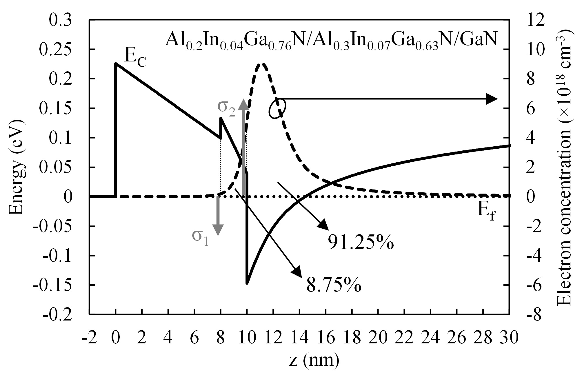
For the first time, a quaternary lattice-matched layer structure based on employing a bilayer barrier has been proposed for improving the carrier confinement in the channel of enhancement-mode AlInGaN/GaN HFETs. Using a commercial self-consistent Poisson-Schrödinger solver, Nextnano, electronic properties of the proposed hetero-structure, including the sheet charge density and carrier confinement on the GaN side of the hetero-interface, were evaluated. Based on these evaluations, it was shown that while the proposed layer structure substantially improves the carrier confinement in the GaN channel layer, it also upholds the merits of employing a lattice-matched barrier towards achieving an enhancement-mode operation. According to the presented simulations, in terms of maintaining the required positive threshold-voltage for the enhancement-mode operation, it is also shown that the proposed layer structure substantially outperforms the quaternary AlInGaN/GaN HFETs employing a thin AlN spacer layer. The outcomes of this research project were published in Journal of Applied Physics on June 2017.
Theoretical evaluation of two 2DEG characteristics of quaternary AlxInyGa1–x–yN/GaN hetero-junctions
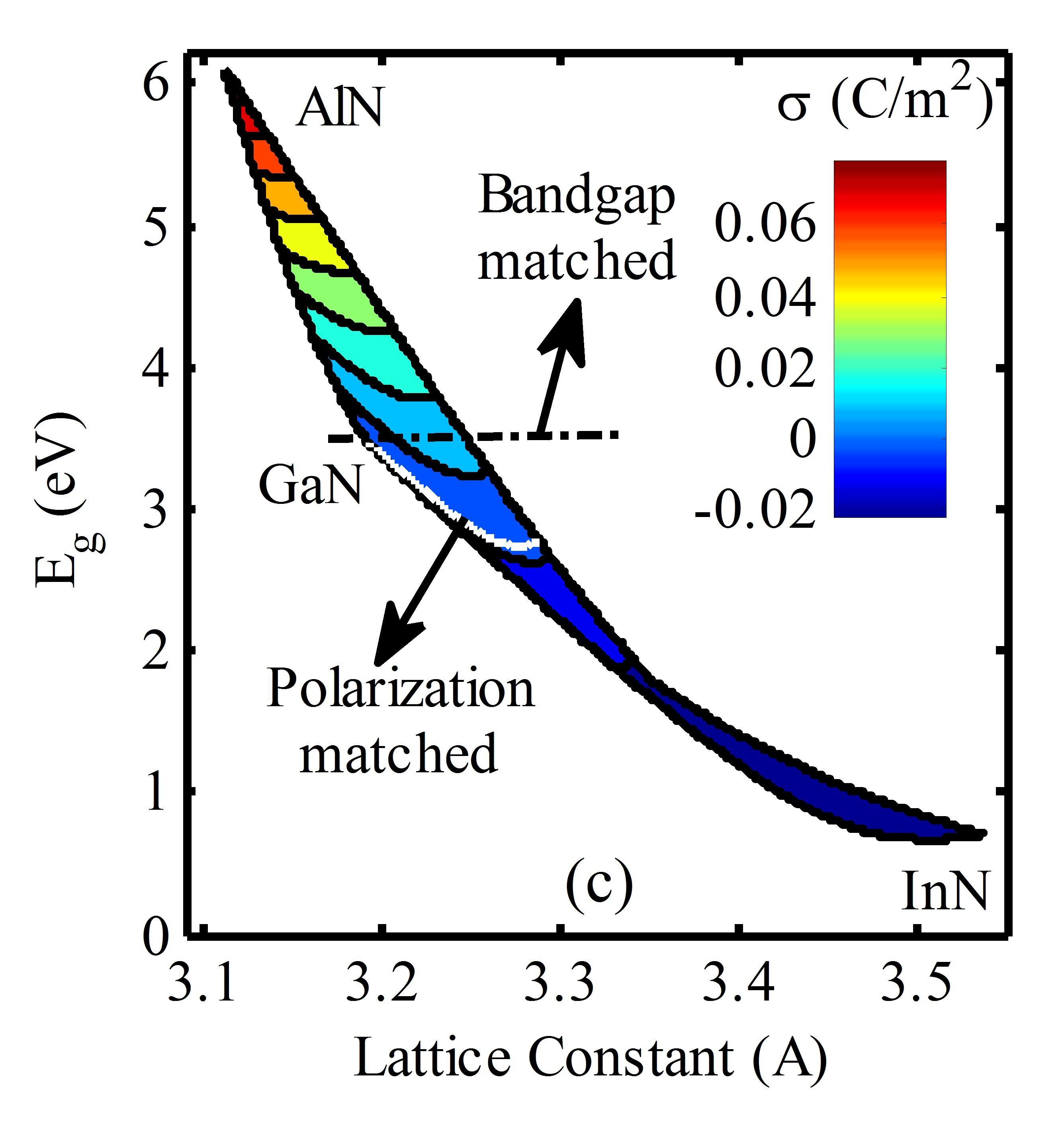
The two-dimensional electron gas (2DEG) characteristics of gated metal-face wurtzite AlInGaN/GaN hetero-junctions including positions of subband energy levels, fermi energy level, and the 2DEG concentration as functions of physical and compositional properties of the hetero-junction were theoretically evaluated using the variational method. Founded on the presented model it is confirmed that the enhancement-mode quaternary AlInGaN/GaN can be realized using polarization engineering of the barrier layer. For the first time, this study revealed that in contrary to the previously claimed possibility of offering polarization-matched quaternary hetero-junctions while retaining the large bandgap of the barrier-layer and the resulting proper carrier confinement, this structure is not capable of implementing this twofold characteristic simultaneously. The result of this study expressed that, although exact matching of polarization is not possible, quaternary barriers can still help desig n devices with low interface polarization charge. The outcomes of this research project were published in Journal of Applied Physics on Apr. 2016.
Modeling and Simulation of InP/InAlGaAs/InP Single Quantum Well Transistor Laser in Ultra-Violet Band
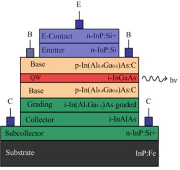
The charge control model and rate equations were used for the first time to glean the optical frequency response of a long-wavelength heterojunction bipolar transistor laser. For a 1.56 µm N-InP/p-InAlGaAs/N-InP fabricated transistor laser with a single quantum well, the optical bandwidth is estimated using this model. The effects of base width on the optical bandwidth and resonance peak of frequency response have been investigated in this study. The result of this study was published in Optical and Quantum Electronics on May 2012.