Short Bio
Kaveh received the B.S. and M.S. degrees from the Amirkabir University of Technology, Tehran, Iran, in 2009 and 2011, respectively, and the Ph.D. degree from Concordia University in 2018, all in electrical engineering. He is currently pursuing the Postdoctoral fellowship with the Photonic DataCom team, McGill University, Montreal, QC, Canada. His research is on development of photonics integrated circuits and systems for modern computing platforms, micro-fabrication of semiconductor devices, modeling and characterization of III-nitride HFETs.
Silicon Photonics MDM PDK
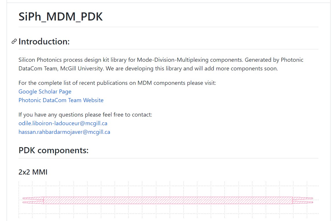
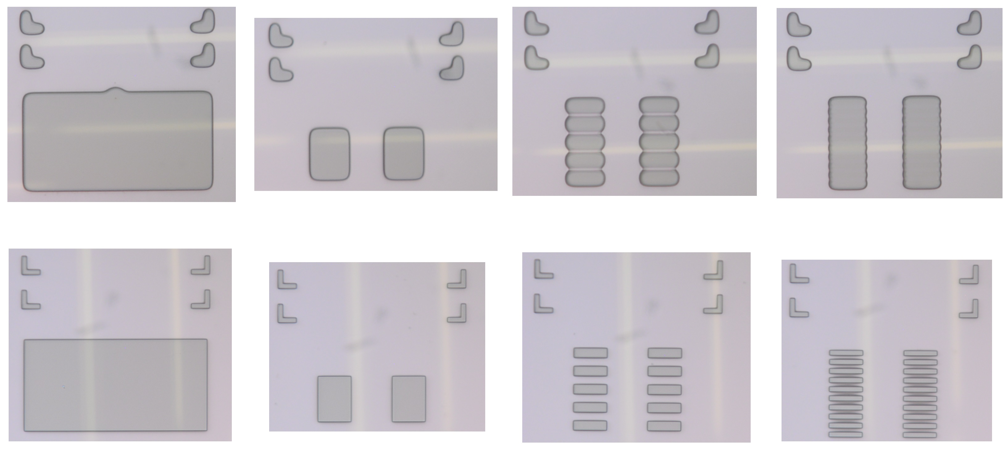
We provide an open access Silicon Photonics PDK for Mode-Division-Multiplexing components. This library includes MMIs, mode Mux/deMuxs, mode sensitive and move insensitive phase shifters, and multimode S-bends. We are developing this library and will add more components soon.
Brief Review of Research Projects
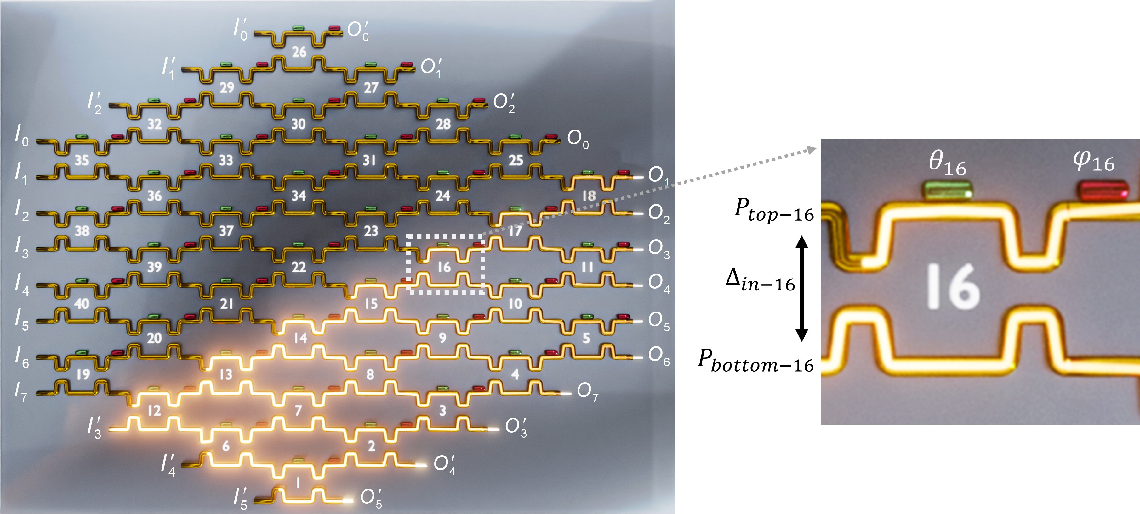
We recently developed a novel mesh of interferometers called "Bokun" mesh. Indeed, the Bokun mesh is a truncated Diamond mesh with the middle optical inputs/outputs (I/Os) used as the main optical path and the peripheral I/Os for calibration purpose only. It can also be
considered as an extended version of Clements mesh with those additional MZIs at the top and bottom of the structure providing diagonal I/O paths for each individual MZI. See more details here .
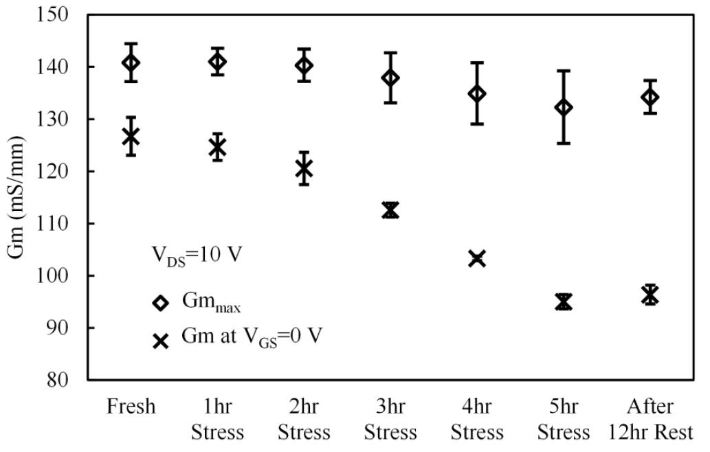
Now you can explore my Github repositories to find several projects on modeling and microfabrication of III-nitride (AlGaN/GaN and AlInGaN/GaN) HFETs, including:
- MATLAB files for physics based simulations of Gate-Leakage and 2DEG characterization of GaN-channel HFETs
- Plenty of experimental data extracted from characterization of various GaN HFETs
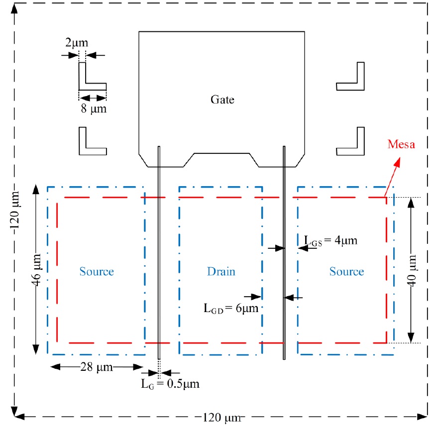
- Details of process recipes developed for microfabrication of submicron gate III-Nitride (AlGaN/GaN and AlInGaN/GaN) HFETs using optical and electron beam lithography (EBL).
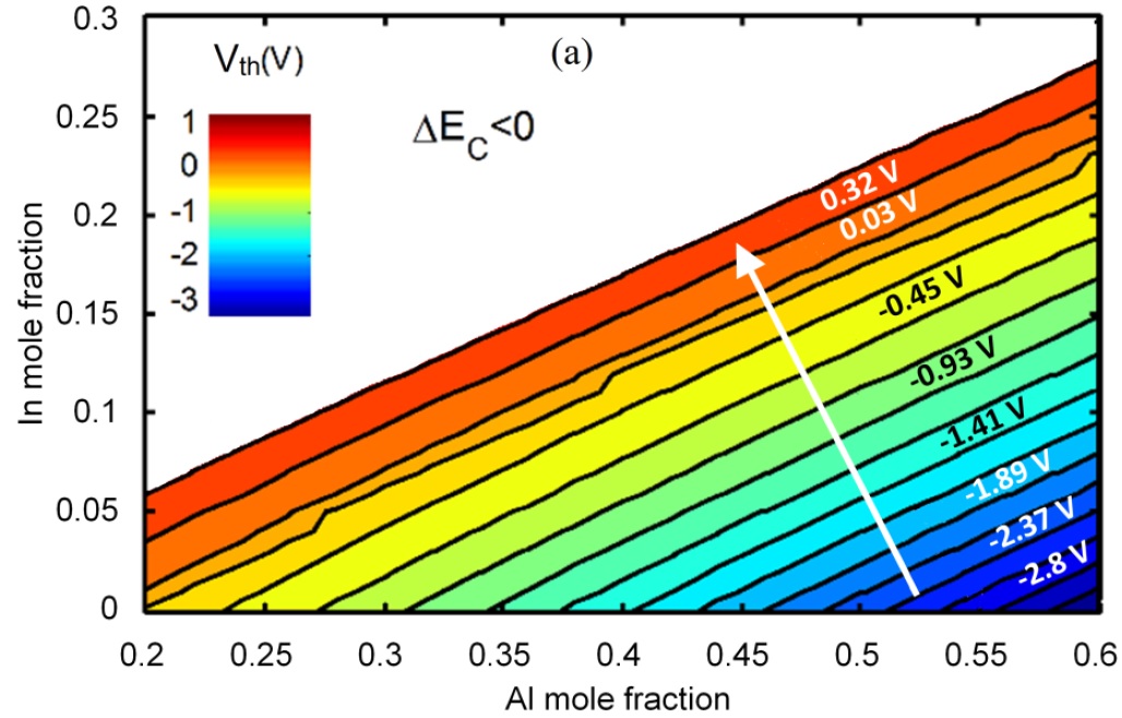
- Simulation codes and output data of quantitative assessment of the gains of employing the bilayer lattice-matched AlInGaN barrier for improving the channel carrier confinement of enhancement-mode quaternary III-Nitride HFETs using the commercial self-consistent Poisson-Schrödinger solver Nextnano
- CAD and run files for EBL using Nanometer Pattern Generation System (NPGS) and TESCAN MIRA3 SEM
- Details of a developed process recipe for EBL using ma-N 2400 negative photo resist for high resolution mesa etching with nanometer feature-sizes.
Check my Github and feel free to use the data for completeing your course projects or developing your research projects. Permission is required for non-academic use. Please do not hesitate to contact me if you need more information.